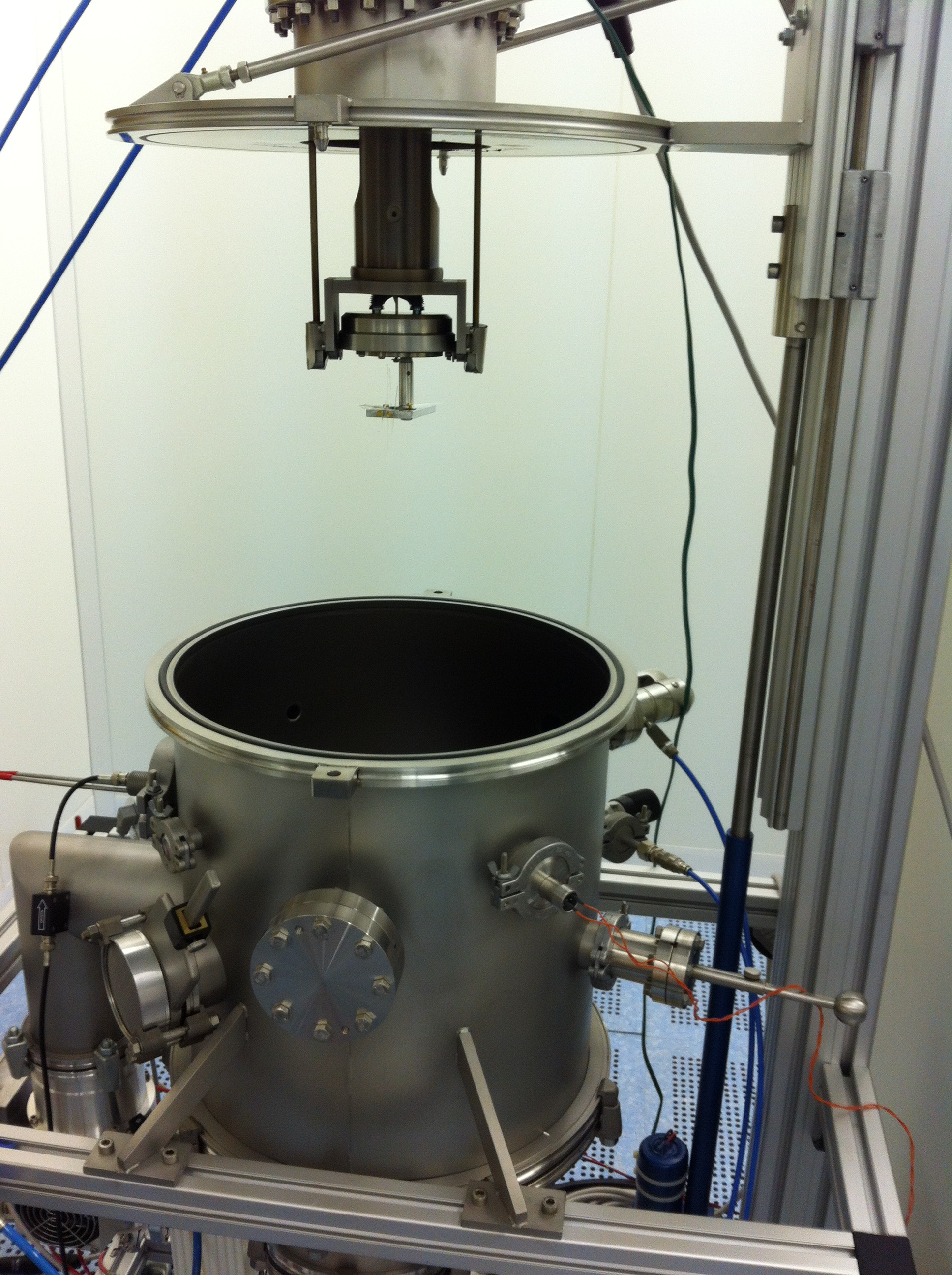
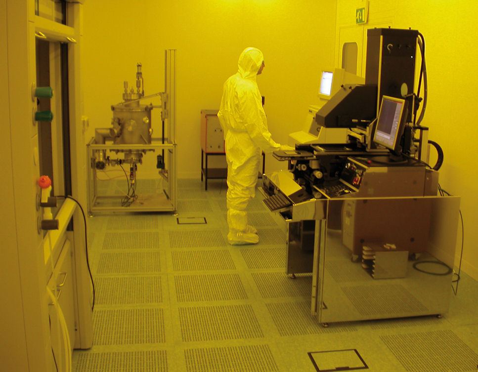
Cleanroom
The Cleanroom Facility is a shared multi-user environment of Class 100/Class 1000 (ISO 5 and 6) level space.
Tool sets and processes complement research in the chemical and physical labs enabling unique capabilities in the pursuit of controlling and manipulating materials at the microscale.
The two-class-1000 clean rooms are equipped with optical tables, microscopes, another profilometer, and are mainly conceived for the characterization and assembly of optoelectronic components.
If you are interested in using the clean room environment and facilities please contact us.
Resources
- A 2-source magnetron sputtering system for metallic and dielectric thin films deposition
- A Reactive Ion Etching (RIE) system
- A stylus profilometer for topography and surface roughness measurements on thin films and bulk substrates
- A chemistry laboratory hood
Contacts:
- Dr. Stefano Pelli, s.pelli@ifac.cnr.it
- Dr. Gualtiero Nunzi Conti, gnc@ifac.cnr.it
Technologies
– Microfabricationsof fiber optical taper, whispering gallery mode microdevices
– Set-up to fabricate and polish microdisks with high quality factor
– Polishing of waveguides and microdevices
– Characterization of materials and devices (integrated, in fiber, micro-optical) by laser sources
– Arc discharge systems to fabricate microdevices
– Thermal furnace for ions exchange process and annealing
– Fiber gratings UV writing system by excimer laser
– Laser source at Argon
– Laser sources at Ti:Sapphire (CW and pulsed)
– Semiconductor pump laser tunable at center wavelength of 980 nm and 1480 nm
– Fiber laser with bandwith less than KHz
– Wideband sources
– Detectors
– Navitar systems
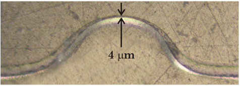
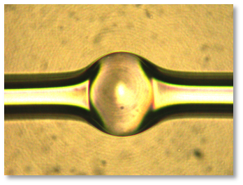
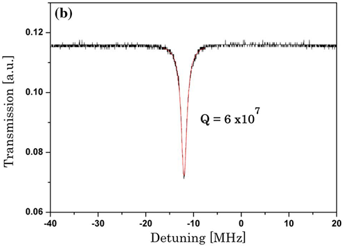
Microbubble resonators
Contacts:
- Dr. Gualtiero Nunzi Conti, gnc@ifac.cnr.it
- Dr. Daniele Farnesi, d.farnesi@ifac.cnr.it
- Dr. Gabriele Frigenti. g.frigenti@ifac.cnr.it
_________________________________
- Fabricated by arc discharge
- High Q-value up to 6*107 at 1550 nm
- Wall thickness 4 micron
For sensing applications this geometry offers:
- external optical coupling
- internal (intrinsic) microfluidics
- 3D confinement vs 2D of LCCOR
Publications
- S. Berneschi, D. Farnesi, F. Cosi, G. Nunzi Conti, S. Pelli, G. C. Righini, and S. Soria, “High Q silica microbubble resonators fabricated by arc discharge," Opt. Lett. 36, 3521-3523 (2011)
- G. Nunzi Conti, A. Barucci, S. Berneschi, M. Brenci, F. Cosi, D. Farnesi, S. Pelli, G. C. Righini and S. Soria, “Coupling approaches and new geometries in whispering-gallery-mode resonators", Proc. SPIE 8236, 82360V (2012); http://dx.doi.org/10.1117/12.909596
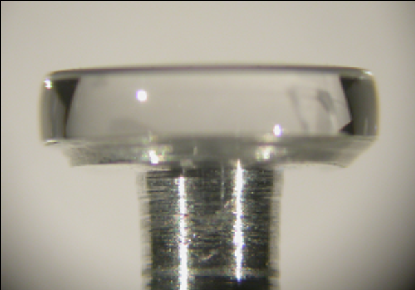
Fabrication of LiNbO3 disks
Contacts:
- Dr. Gualtiero Nunzi Conti, gnc@ifac.cnr.it
- Dr. Daniele Farnesi, d.farnesi@ifac.cnr.it
- Lithium niobate disks of 5 mm in diameter were made from commercial 3†x 1 mm thick Z-cut lithium niobate wafers by core drilling a cylinder and thereafter polishing the edge into a spheroidal shape.
- We have optimized the polishing procedure of crystalline disks using a home-made lapping station.
- The almost spherical profile is obtained either by a suitable preform having the desired curvature or through a rotational stage whose pivot point can be finely adjusted.
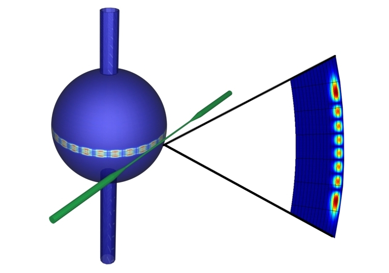
Spherical microresonators
Publications
- Pasquardini, L., Berneschi, S., Barucci, A., Cosi, F., Dallapiccola, R., Insinna, M., Lunelli, L., Conti, G. N., Pederzolli, C., Salvadori, S. and Soria, S. (2012), Whispering gallery mode aptasensors for detection of blood proteins. J. Biophoton.. doi: 10.1002/jbio.201200013
- Soria S., Berneschi S., Brenci M., Cosi F., Nunzi Conti G., Pelli S., Righini G.C., Optical Microspherical Resonators for Biomedical Sensing, Sensors 2011; 11(1):785-805
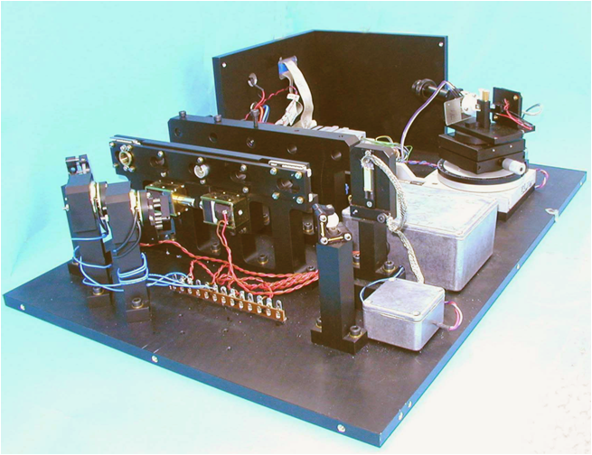
COMPASSO
an instrument to test and characterize waveguides and thin films
COMPASSO is based on m-line spectroscopy and prism coupling technique, and it allows the rapid measurements of waveguides parameters and thin films
Applications
– Direct measurements of sublayer refraction index and cromatic dispersion
– Refraction index, thickness or refractive index profile of thin films
– Direct measurements of propagation constants (effective refractive index) of planar waveguides at 5 different wavelength (635 – 1550 nm)
Contact person:
- Dr. Stefano Pelli, s.pelli@ifac.cnr.it
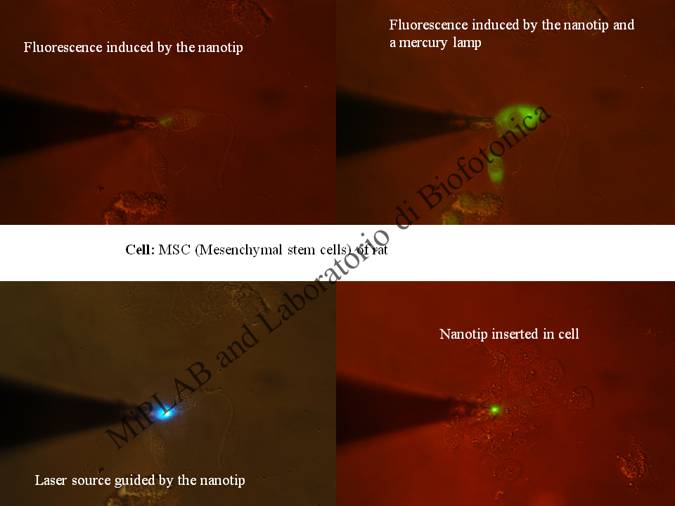
Fiber optical Nanotips fabrication
In our laboratory we are able to fabricate by several chemical etching methods fiber optical nanotips for SNOM, AFM and biological applications.
The nanotips can be obtained by single and multimode fiber optical.
The nanotips have a distal end less than 100 nm.
We are willing to share samples for research purposes.
Contacts:
- Dr. Stefano Pelli, s.pelli@ifac.cnr.it